
Innoswitch working
Hi,
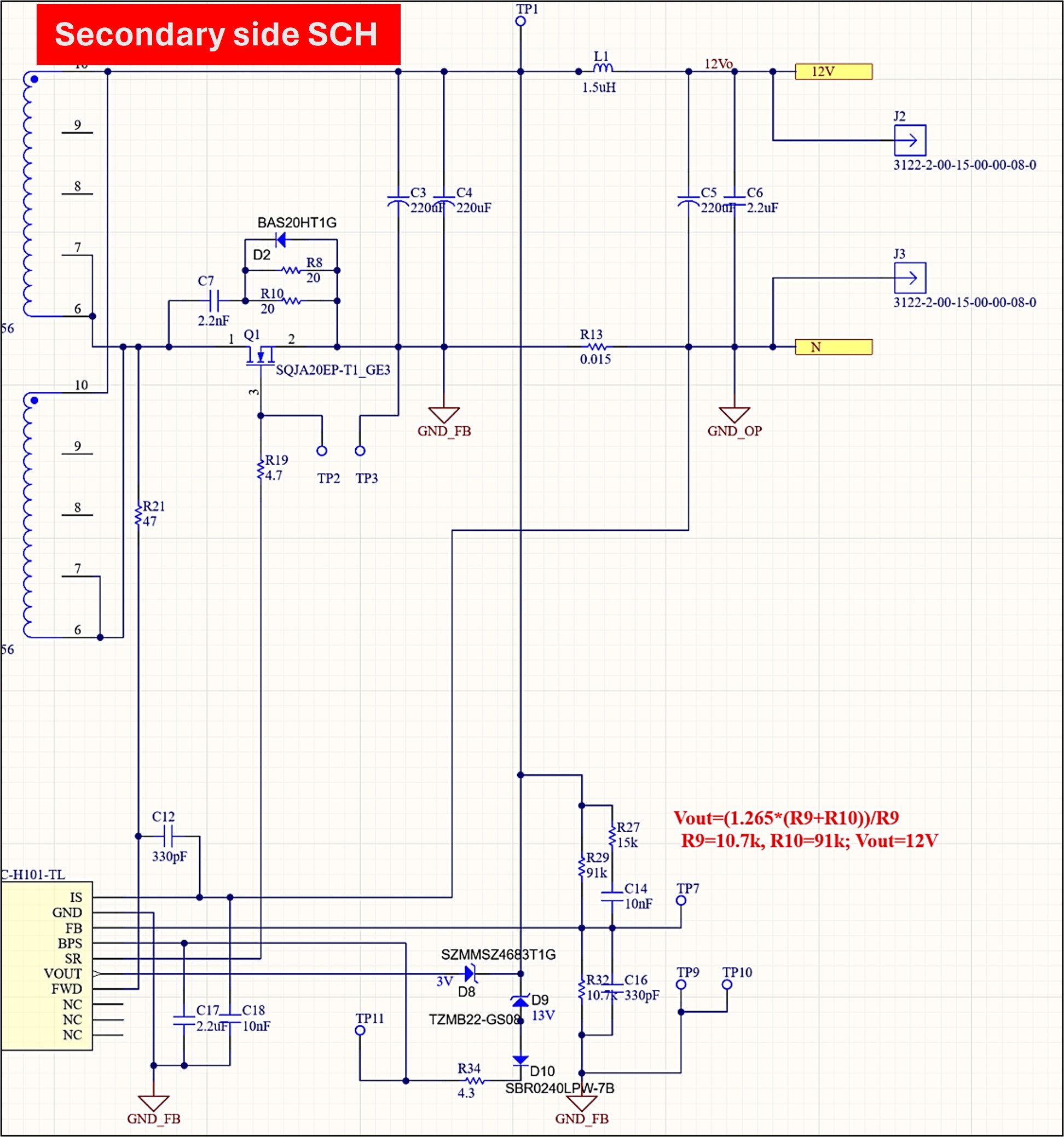
I'm using INN3165C for my wide-input range flyback. My secondary looks very similar to that of DER-717 (attached image)
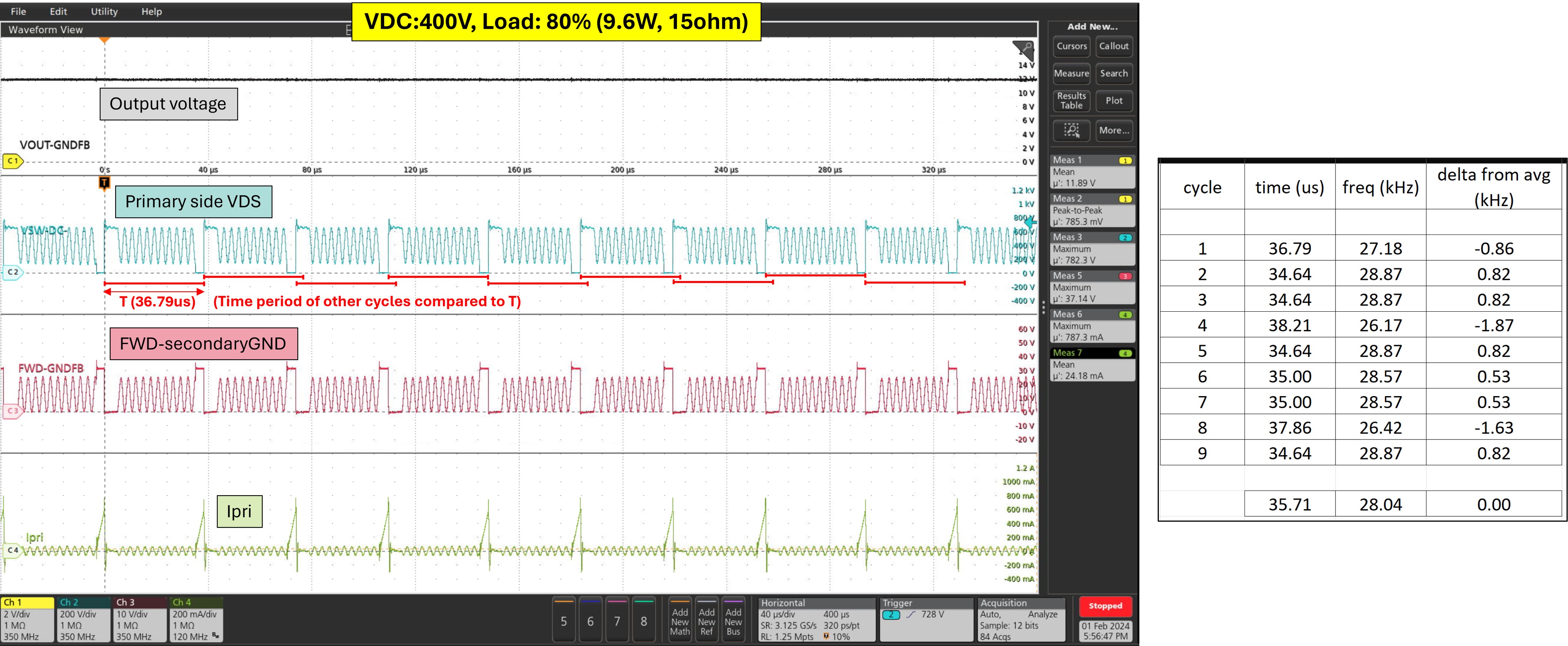
1. At a fixed input voltage and load, I observed the switching frequency changes in a +-2kHz band. (attached image). Is this some feature of the innoswitch controller? From my understanding of closed-loop flyback, frequency jumps (when every input is constant) is indicative of oscillations in closed loop response.
2. I noticed a feature called Jitter (to reduce EMI). What is this and which parameter does it affect? Why is it implemented? How does it work?
Datasheet says "The normalized current limit is modulated between 100% and 95% at a modulation frequency of fM. This results in a frequency jitter of ~7 kHz with average frequency of ~100 kHz". What does this mean? How is the 7kHz value calculated? What does "average frequency of 100kHz" mean? (Is this jitter the reason I'm seeing frequency variations mentioned in previous question?)
3. How does the controller set its switching frequency? I understand from the datasheet that it operates at 25-95kHz depending on load, startup, steady state condition, and that there's a recommended full load operating freq. But how does the IC set a switching freq - what logic/math does it use?
4. When does the controller decide to switch the primary - which event triggers switching under normal operating conditions (or. eg. current exceeding a certain value, VFB dipping below a threshold). How does the controller decide its duty?
Files
| 첨부 파일 | 파일 크기 |
|---|---|
| innosw forum2.jpg | 528.41 KB |
| innosw forum1.jpg | 921.36 KB |
댓글
Thank you, this was helpful.
1.In my case, I noticed, as converter slips further into DCM, the primary on time decreases to few tenths of us. This is much lower than the "minimum secondary off time" mentioned in the datasheet. How is this possible?
2. the inductor I've chosen isn't optimised I feel because the converter operates in DCM for 99% of the operating points. For a fixed load, as input voltage increases, DCM further increases. Beyond a certain input voltage, the controller stops working. Is this fault because of too little Ton of primary?
3. What other situations can cause controller to fault as input voltage increases (load constant through out) ?
Hi pppp,
1) There is no mention of “minimum secondary off time” in the datasheet. Assuming you meant “minimum off time”, this defines the time between the primary switch turns off and when the secondary can send a switching cycle request again. It is basically the minimum primary t_off of the device.
2 & 3) If the power supply stops switching, you may need to check the resistors connected between the V pin to the positive terminal of your input. If the current through the resistor reaches Iov+ (115 uA), the device considers this as an input overvoltage event and power supply will stop switching until the current though the resistor reaches the normal operating value in the datasheet. If you wish to quickly confirm if the input overvoltage protection causes the response that you observe, you can short the V pin to the S pin of the InnoSwitch3-CE IC. Doing so bypasses the input undervoltage/overvoltage protection feature. You just need to make sure that your components can handle the high voltage stress, specifically the InnoSwitch3-CE primary switch and the SR diodes/FETs.
I hope to have answered you questions. If you wish to ask questions regarding a different topic, kindly create a new post on PI Forum and we will assist you. Thank you.
Thank you Pi-Prowler, you replies are helping fill in the gaps in my understanding of the IC.
1) apologies for my misunderstanding. What is the range on min Ton of primary?
2) in my design, V pin shorted to S. What other signals should I check and compare against?
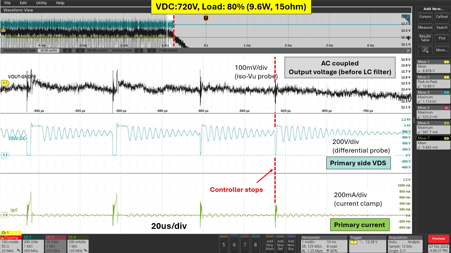
I'm attaching the shutdown event waveform
| 첨부 파일 | 파일 크기 |
|---|---|
| innosw forum3.jpg | 274.49 KB |
Hi Pranit,
If you are using INN3165C, you are operating way above the maximum rating of the IC. The peak drain voltage the device can handle is only 650 V. Based on your waveform, the primary drain voltage reaches above 1 kV already. This is beyond the safe operating region of the device and most likely it is trying to protect itself to prevent further damage.
You may need to limit your input specifications or use a different device for your application. InnoSwitch3-AQ Family devices are used in automotive applications and have products with a primary SiC switch that is rated up to 1700 V. Just note that the transformer design must be updated because the Innoswitch3-AQ Family generally has a higher ILIM and that may risk saturating the transformer. I have attached the link below for the datasheet.
https://www.power.com/sites/default/files/documents/innoswitch3-aq_family_datasheet.pdf
Thank you for using PI Forum.
Oh sorry for not giving the bigger picture. The flyback under test incorporates a StackFET like ckt to operate at higher voltages (2kV intended). The tranformed also has been designed accordingly.
I cannot share much details on the forum as its a confidential design, but its been validated in simulations along with load, line variations. Peak voltage observed on the innoswitch DS is much lower than 650V.
Going back to previous questions -
1.what is the range on min Ton of primary?
2) in my design, V pin shorted to S. What other signals should I check and compare against?
Thank you. I'm sorry for the confusion
There is no minimum on time for the primary switch on the datasheet, only the maximum turn on time.
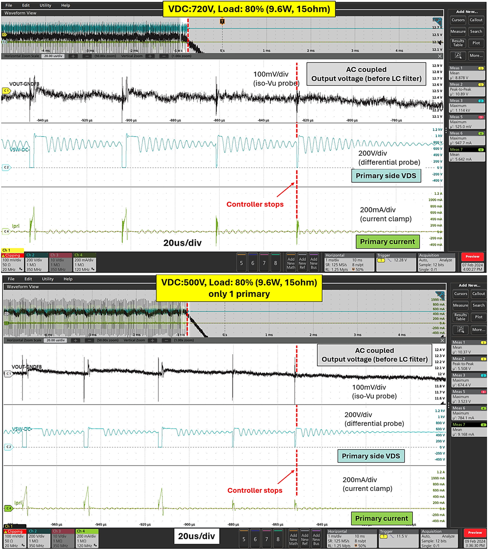
In the latest waveform you captured, it looks like the primary switch turns off prematurely in the last 2 cycles. You may need to check if the necessary current is being supplied to the BPP pin and that its voltage does not drop below the typical value. Monitoring the SR DS and GS voltage can also give you more information regarding the unexpected shutdown event.
For other protection features, you can check the SR Short protection and SOA protection in page 5 of the Innoswitch3-CE datasheet. If the design has a primary bias circuit and primary side output ovp circuit, you can check the current passing through the BPP pin to confirm if it goes above Isd (7.5 mA), causing the unit to latch off. You can also check the thermal performance of the device to see if Over-Temperature Protection (OTP) is being triggered.
Update: I replaced the existing inductor with one having half the magnetising inductance and observed the operation.
This time the shutdown occurred at 500VDC (200V lower than previous result). Is the shutdown related to Lm value?
Also, how to calculate Lm value for a given application? Is there a app note that I can follow? (PI Expert isn't allowing me to input proceed further when I'm inputting INN3165C as the part)
| 첨부 파일 | 파일 크기 |
|---|---|
| image (12).png | 781.39 KB |
Hi Pranit,
I don't have enough information on your design to provide further analysis on the event. If you need a reference for a flyback design with ultra wide input, you can look at DER-712. I've provided the link below.
Regarding PI Expert, you can use PI Xls to design your transformer. It will still allow high input voltages for INN3165C and will only show a warning regarding the peak primary drain voltage.
I went through the design reference and it is similar to my design. I will go through the PI XIs software for xfmer design. Thank you :)
In a previous app note you shared, AN-72. I noticed the SRFET switching wfm (pg 18). If I understand it right, the SRFET turn-on is ZVS, and turn-off is dependent on SR-FET VDS during conduction period. I observed the same wfms in my setup and I noticed, in some waveforms, non-ZVS behaviour during turn-on, and premature turn-off (maybe).
In some cycles, the SRFET waveforms are as expected (AN-72, pg. 18), in some cycles they are not. If I understand the working right, the IC senses the drain-src voltage via the FWD pin and turns-on the SRFET after the first zero-crossing of FWD voltage. The SRFET is turned OFF after VDS reaches zero during conduction cycle (pg. 18). I'm not able to understand, why the SRFET on time is varying so much between cycles. Could you provide some insights/potential causes?
| 첨부 파일 | 파일 크기 |
|---|---|
| innosw forum4.jpg | 1.15 MB |
| innosw forum5.jpg | 1.05 MB |
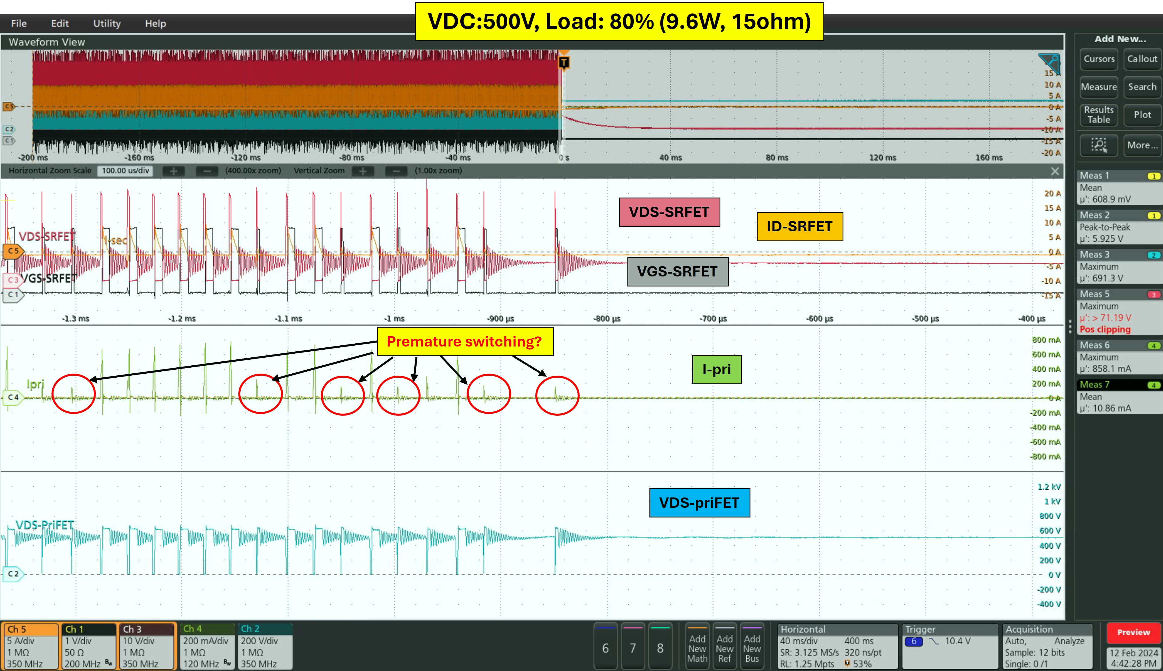
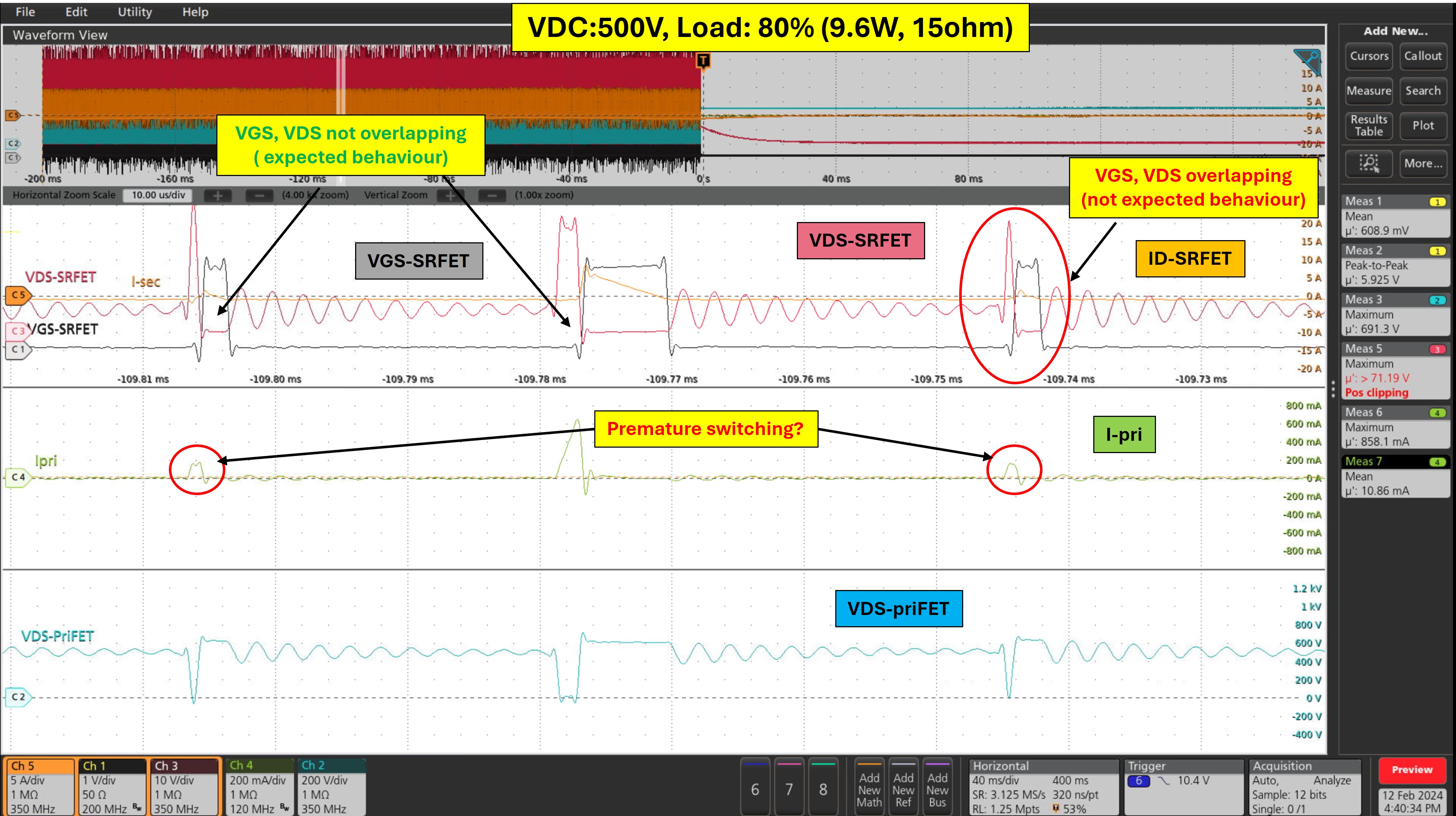
Hi pppp,
1 & 2) Given that both input and output parameters are constant, the change in switching frequency is most likely due to the jitter. The jitter works by modulating the primary drain current limit by a certain frequency. The datasheet explains that when operating at 100 kHz switching frequency, the peak drain current will oscillate from 100% to 95% of the current limit (defined as "ILIM" or "ILIM+1" in the datasheet). This oscillation is fm, which is typically 1.25 kHz. The oscillation of the peak drain current effectively means that the flyback energy per switching cycle will oscillate at a specific range, which in effect makes the switching frequency oscillate at around 93 kHz to 107 kHz. When operating at a different switching frequency, jitter is still implemented, but will have a different change in the switching frequency. This jitter is mainly to reduce EMI by spreading the EMI noise around the average switching frequency instead of being concentrated at that point only.
3 & 4) Figure 4 in the InnoSwitch3-CE Family datasheet shows the block diagram for the secondary side controller. The FWD pin voltage, output voltage information from the FB pin, and the output current information from the IS pin will dictate when switching cycle requests to the primary is needed. The switching frequency is not directly set, but rather an effect of when the switching cycle request happens. It is up to designer to set the switching frequency based on the transformer design and input/output conditions.
Regarding the duty cycle, after the switching cycle request, the primary switch turns on until either the drain current reaches the specified current limit (will depend on ILIM or ILIM+1 and the scaling factor in Figure 6) or until the maximum primary on time (ton(max) = 14.6 us) is reached.
I've attached the datasheet for Innoswitc3-CE and the design guide for power supplies using InnoSwitch3 Family devices (AN-72).
I hope that I have provided answers to your concerns. Thank you for using PI Forum.